
IBM might seem like a company that is currently on the fringes of the tech world’s popularity. But the American brand surprised everyone and everything by announcing now about the 2 nm chip.
Thus it is the first company in the world to develop the first chip made using 2nm lithography.
IBM announced the 2nm chip
The giant IBM Corporation Advertise This Thursday, May 6, it is the first company in the world to develop the first chip made in a 2 nanometer (nanometer) process.
After a lot of talking in Taiwanese TSMCAfter all, it was the American who first took this giant step.
According to IBM, this chip is designed to be 45% faster and 75% more efficient than the 7nm chip. The brand adds that these semiconductors offer several benefits, including a reduced carbon footprint in data centers, where they account for 1% of all global energy use.

Additionally, the chip could also help speed up the functionality of laptops, while providing faster processing in applications. It will also help speed up language translation and speed up Internet access.
IBM's 2nm semiconductor can quadruple the battery life of smartphones, allowing users to charge their devices only every four days. It will also contribute to faster object detection and reaction time in autonomous vehicles.
According to Dario Gill, Senior Vice President and Director of IBM Research:
The innovation reflected in this new segment is essential to creating new and more robust technology platforms that can help our society deal with major challenges, from climate change and sustainability, to food shortages.
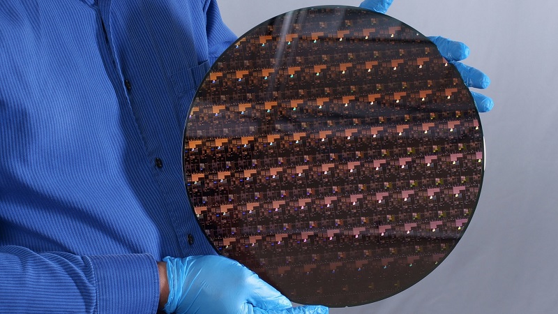
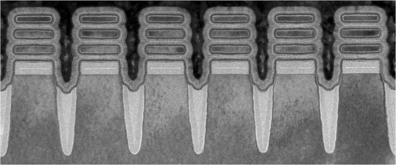
A chip with 50 billion transistors
IBM's new 2nm chip contains 50 billion transistors built into a segment the size of a nail. The company says the construction is the result of the nanopaper technology, which made it possible to develop the chip in as little as 4 years, after the announcement of the 5 nm chip.
Semiconductors were developed at the IBM laboratory located in Albany, New York, USA. There, the scientists collaborated with partners from the public and private sectors, such as Samsung and Intel.
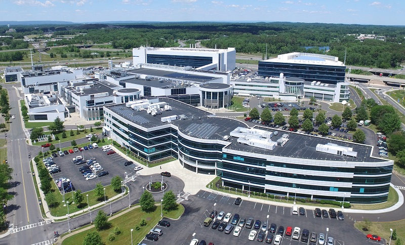
IBM lab in Albany, New York, USA
Thus this was an important step in the nanotechnology sector, which will certainly bring major contributions to the development and innovation of the technology we know today.

“Wannabe internet buff. Future teen idol. Hardcore zombie guru. Gamer. Avid creator. Entrepreneur. Bacon ninja.”